


Home > Product Range > PCB > PCB Design > PCB Design
|
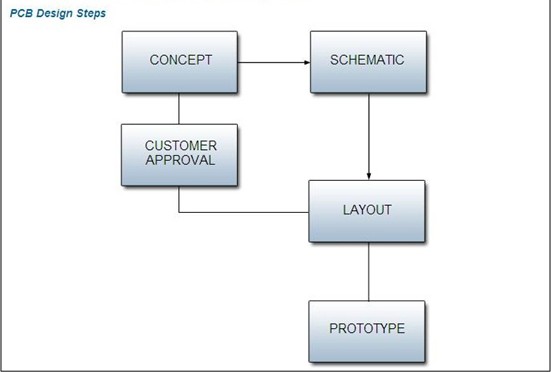
PCB Design & Layout If you have a schematic or a drawing, but do not have time or tools to complete the design, we can help you. With your schematic, we can take your design to completion in the following steps. · Design component footprints · Establish PCB outline · Setup design rules, e.g. spacing, impedance, etc. · Place components · Perform manual route traces on critical components, e.g. clocks, power, sensitive analog parts, etc. · Perform auto router · Run design rule checker · Produce Gerber files We can also take your design to reality with PCB fabrication and PCB assembly services.
Please contact atsale@chinapcba.comif you need urgently quote. We will reply you within 2hours after received your email. |
Product Range
 PCB Design
- ---PCB Design
- ---PCB Layout and Setup Tips
- PCB Prototype
- PCB Production
- PCB Picture
- ---Communications PCB
- ---Industrial Equipments PCB
- ---Consumer Electronics PCB
- ---Auto Electronics PCB
- ---Digital Electronics PCB